

Product Category
Brands


Product Category
Brands


Product Category
Brands


Product Category

Brands


Product Category
Brands


Product Category
Brands


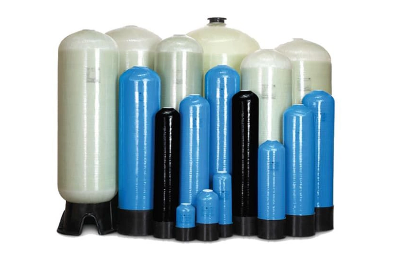
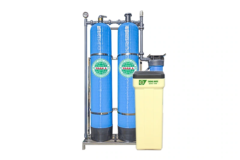
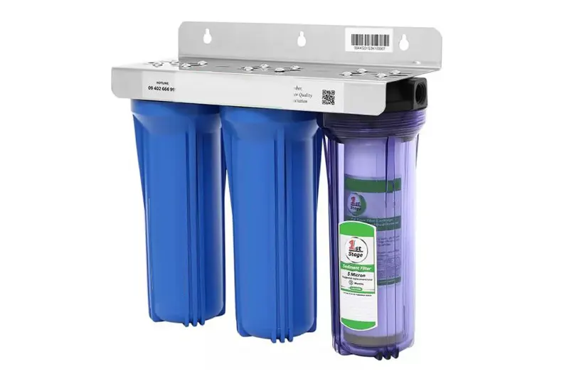
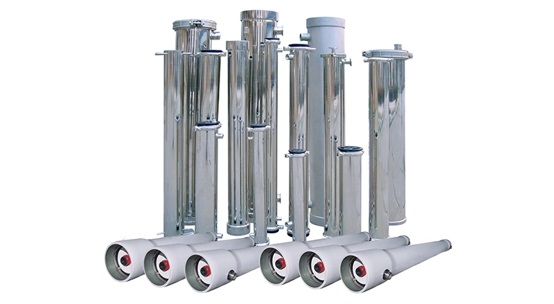
 Water Filter Columns
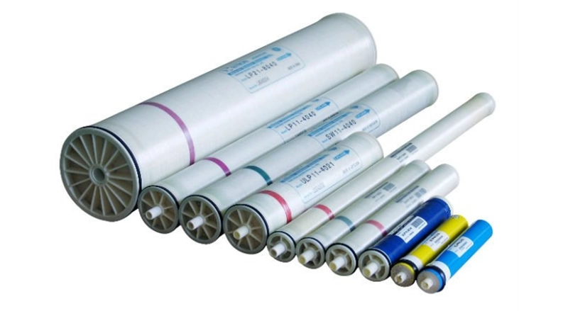
 Water Filtration Membranes
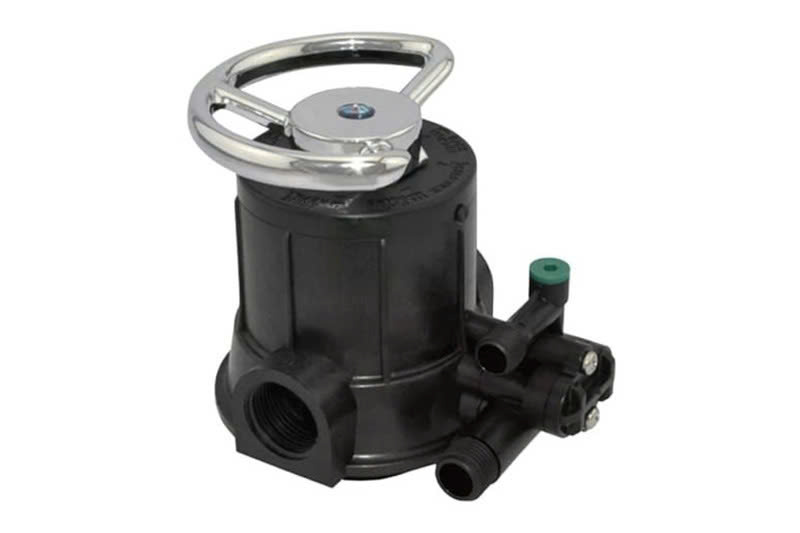
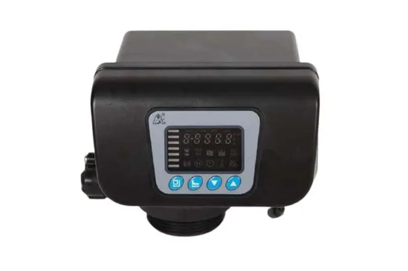
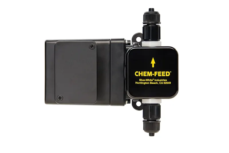
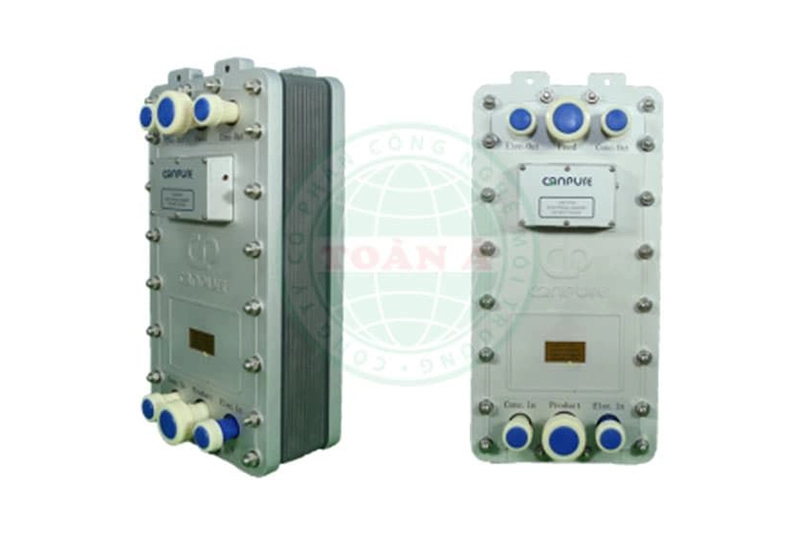
 Control Valves
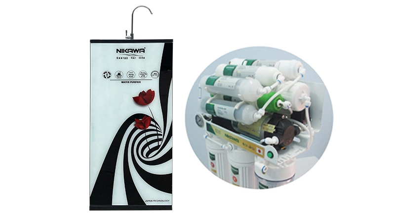
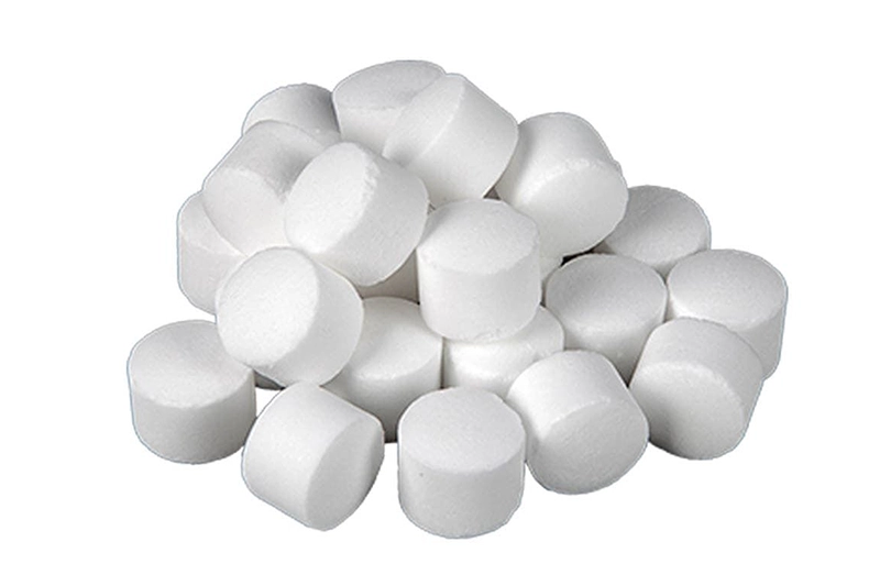
 Water Filter Cartridges
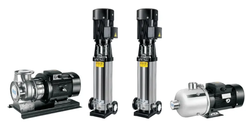
 Water Pumps
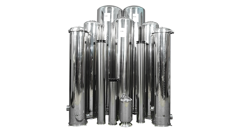
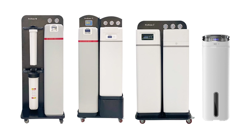
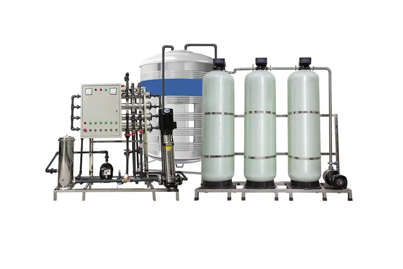
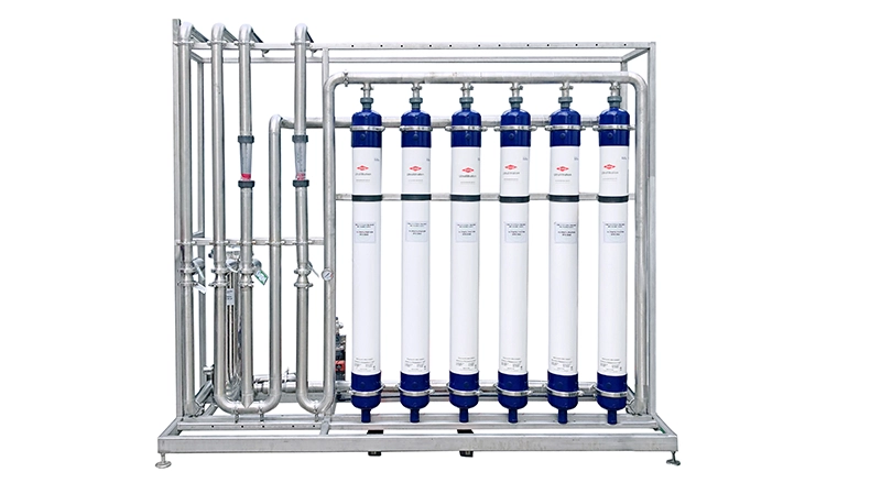
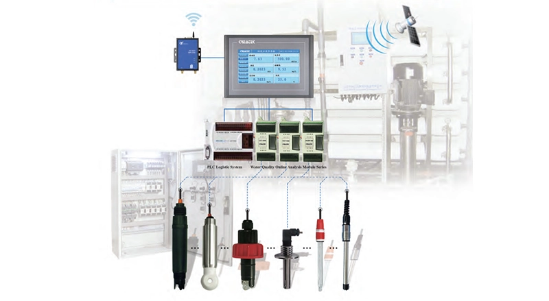
 Water Filtration Equipment
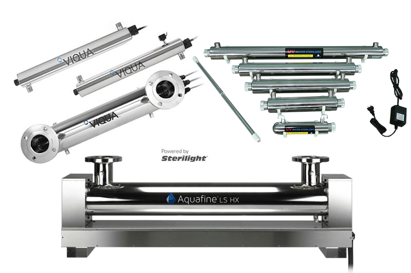
 Water Filtration Components
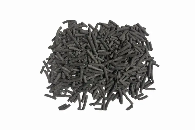
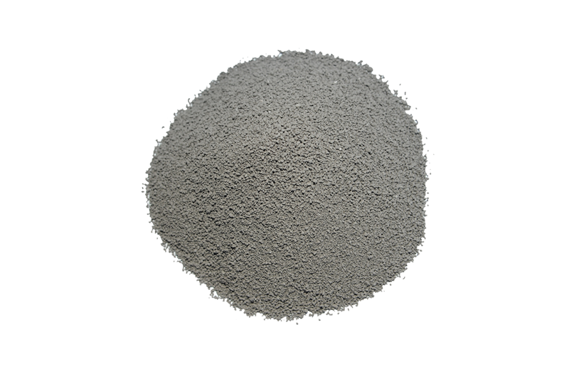
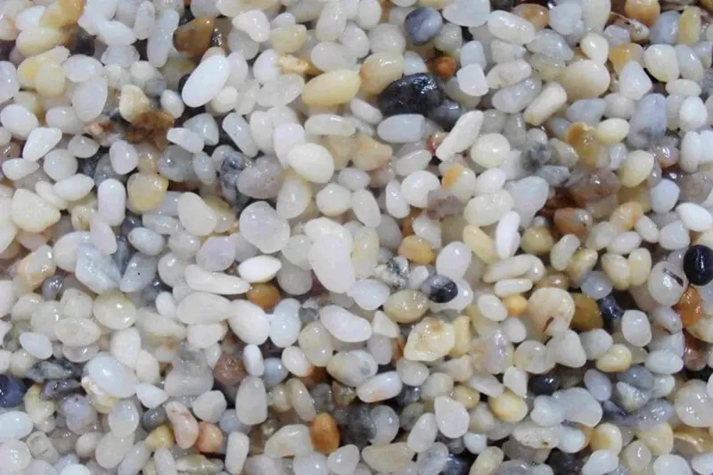
 Water Filtration Materials
 Heat Pump Water Heaters
Your cart is empty !

Semiconductors Solution
Update: 02/01/2025
Share:


Content


Semiconductors Solution
Update: 02/01/2025
Share:
The process of treating semiconductor manufacturing wastewater includes collecting wastewater and treating it through various steps to remove harmful substances and meet the specified wastewater quality standards.
What is semiconductor manufacturing wastewater?
Semiconductor manufacturing wastewater is the type of wastewater generated during the production of semiconductors. Typically, this wastewater source can be found in manufacturing plants that produce electronic components or technological devices.
Semiconductors are materials that have the ability to conduct electricity at an intermediate level. That is, they are half conductive and half non-conductive. Specifically, at room temperature, they conduct electricity like ordinary metals, but at low temperatures, they act as insulators.
This material is commonly found in the electronics industry, in all products using digital technology, radio waves, etc.
Why is it necessary to treat semiconductor wastewater?
Establishing a semiconductor manufacturing wastewater treatment system is a very important task that needs to be focused on. It is not only essential for the environment and people but also crucial for the industry itself, electronic factories, and technology facilities.
- Protecting the ecosystem.
- Protecting public health.
- Ensuring legal compliance.
- Building a brand reputation.
- Maintaining company pipelines and public infrastructure.
Methods of treating semiconductor manufacturing wastewater
Modern technology
Semiconductor wastewater is often difficult to treat, as it is highly colored. In addition, it has high levels of VOCs (volatile organic compounds) and heavy metals. Therefore, treating this type of wastewater requires the use of various methods and technologies. The most common methods are the following 4:
Physicochemical method
This method, also known as the adsorption method, involves using substances such as activated carbon, clay, alum, silica, straw, bagasse, etc. These are compounds that have a good ability to absorb metal ions, thereby removing metal content in semiconductor wastewater.
.jpg)
This treatment method is highly effective, easy to implement, and the adsorption materials can be reused.
Chemical method
This treatment method consists of 2 stages:
Oxidation-reduction and precipitation
- Stage 1: Oxidation-reduction: Using good oxidizing agents such as chlorine, hypochlorite, dichloroisocyanurate, etc. These substances play a role in reducing the toxicity of pollutants in the water and separating them from the water.
- Stage 2: Precipitation: Using alkali chemicals such as NaOH, Na2CO3, lime, etc. to precipitate metals. Then separate them by sedimentation in wastewater.
This is the most common method today as it provides high efficiency. However, it requires a large amount of chemicals.
Using ion exchange method
This is a modern and effective method. Two columns, cationic and anionic, are used to remove heavy metals such as copper, calcium, sodium, chromium, Cl-, SO42-, CN-, NO32-, etc.
This method is easy to implement and does not require a large area. It is suitable for small units and industries.
Biological method
The essence of this method is to use plants, microorganisms that can absorb metals to reduce the metal content in semiconductor wastewater. Typically, water hyacinth, bee pollen, algae, etc., are used.
However, this method is only applicable to light wastewater sources. Additionally, it requires sufficient nitrogen, phosphorus, and trace elements for microorganisms to grow.
Semiconductor wastewater treatment process
Treating semiconductor manufacturing wastewater is the most challenging task. Therefore, the treatment process is relatively complex. In general, it will include 7 stages as follows:
Coarse filtration
Wastewater in the production process will be sent to a trash rack. Here, large solid particles will be retained to prevent blockages in subsequent steps. The wastewater after coarse filtration will be sent to a reception tank, then to a conditioning tank.
Conditioning tank
Here, the wastewater will be conditioned for flow rate and concentration. The entire wastewater will be agitated to prevent sludge settling.
.jpg)
Reaction tank
Here, chemical reactions will take place to change the properties of the wastewater. To treat semiconductor industrial wastewater, NaHSO4, FeSO4 are evenly mixed and rapidly added to the wastewater. The result will be fine sludge that will be transferred to the coagulation process in water treatment.
Coagulation tank
Here, NaOH, CaO will be continuously added to the tank. These substances will act on metal ions and existing sludge in the water. Then, larger sludge particles will be formed for easy sedimentation. The entire mixture will automatically flow through a settling tank.
Intermediate tank
This is the next stage after the settling tank, where wastewater from the settling tank will be transferred to the intermediate tank for pressure filtration. The remaining sludge will be pumped to a separate holding tank for collection and treatment as required.
Pressure filtration
The pressure filtration tank will contain filtration materials such as quartz sand, activated carbon, water filtration stones, etc., to filter out remaining toxic substances in the wastewater. Specifically, soluble organic compounds, trace elements, etc.
The final stage of the wastewater treatment process: Discharge the treated wastewater to the receiving location through the pre-established system.
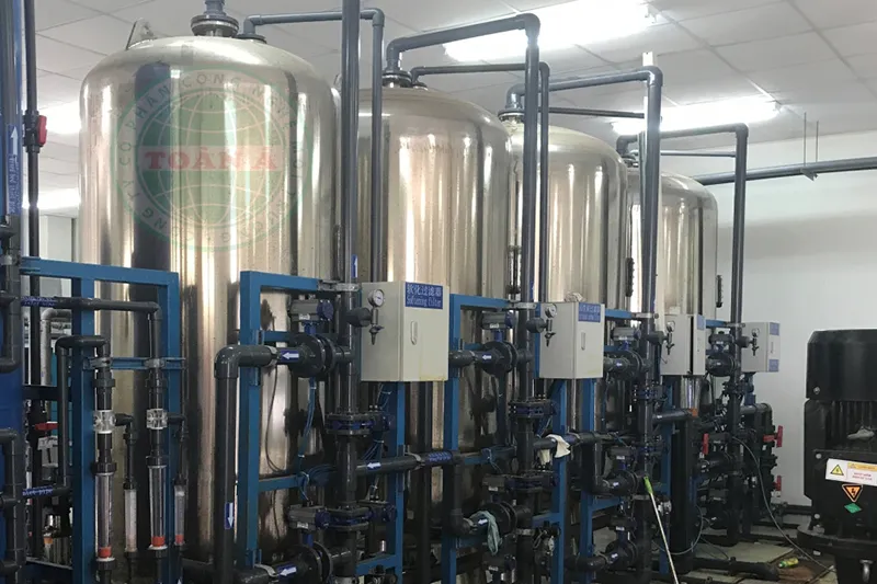
Semiconductor wastewater treatment system at Toan A
Currently, the semiconductor wastewater treatment system at Toan A is being chosen by many people. The system installed by Toan A provides high efficiency in water treatment. Therefore, it serves the industrial sector in manufacturing and supplying technological components and electronic devices.
.jpg)
Toan A builds and develops a semiconductor wastewater treatment system with a quality model, ensuring a clean and healthy environment. At the same time, it can meet the requirements of enterprises in the process of manufacturing electronic equipment and components.
The treated wastewater output when using Toan A's treatment system meets the standards of industrial wastewater treatment with various stages:
- Mechanical treatment.
- Chemical treatment.
- Biological treatment.
- Water filtration.
If you are operating a plant that manufactures components related to technology, using a wastewater treatment system is essential... This action helps ensure that the treated wastewater meets the standards, ensuring the safety of the surrounding environment and compliance with the law.
You can contact Toan A immediately for the most detailed advice on technology, processes, and semiconductor wastewater treatment systems.
Update: 02/01/2025
Share:


 Products
  Solutions
  Project
  News
News